XS40, XSP, and XS95 Board Manual
XESS Corporation
Copyright ©1997, 1998 by X Engineering Software Systems Corporation.
All XS-prefix product designations are trademarks of XESS Corp.
All XC-prefix product designations are trademarks of Xilinx.
ABEL is a trademark of DATA I/O Corporation.
All rights reserved. No part of this publication may be reproduced, stored in a retrieval system, or transmitted, in any form or by any means, electronic, mechanical, photocopying, recording, or otherwise, without the prior written permission of the publisher. Printed in the United States of America.
Limited Warranty
X Engineering Software Systems Corp. (XESS) warrants that the Product, in the course of its normal use, will be free from defects in material and workmanship for a period of one (1) year and will conform to XESS’s specification therefor. This limited warranty shall commence on the date appearing on your purchase receipt.
XESS shall have no liability for any Product returned if XESS determines that the asserted defect a) is not present, b) cannot reasonably be rectified because of damage occurring before XESS receives the Product, or c) is attributable to misuse, improper installation, alteration, accident or mishandling while in your possession. Subject to the limitations specified above, your sole and exclusive warranty shall be, during the period of warranty specified above and at XESS’s option, the repair or replacement of the product. The foregoing warranty of XESS shall extend to repaired or replaced Products for the balance of the applicable period of the original warranty or thirty (30) days from the date of shipment of a repaired or replaced Product, whichever is longer.
THE FOREGOING LIMITED WARRANTY IS XESS’S SOLE WARRANTY AND IS APPLICABLE ONLY TO PRODUCTS SOLD AS NEW. THE REMEDIES PROVIDED HEREIN ARE IN LIEU OF a) ANY AND ALL OTHER REMEDIES AND WARRANTIES, WHETHER EXPRESSED OR IMPLIED OR STATUTORY, INCLUDING BUT NOT LIMITED TO, ANY IMPLIED WARRANTY OF MERCHANTABILITY OR FITNESS FOR A PARTICULAR PURPOSE, AND b) ANY AND ALL OBLIGATIONS AND LIABILITIES OF XESS FOR DAMAGES INCLUDING, BUT NOT LIMITED TO ACCIDENTAL, CONSEQUENTIAL, OR SPECIAL DAMAGES, OR ANY FINANCIAL LOSS, LOST PROFITS OR EXPENSES, OR LOST DATA ARISING OUT OF OR IN CONNECTION WITH THE PURCHASE, USE OR PERFORMANCE OF THE PRODUCT, EVEN IF XESS HAS BEEN ADVISED OF THE POSSIBILITY OF SUCH DAMAGES.
In the United States, some statutes do not allow exclusion or limitations of incidental or consequential damages, so the limitations above may not apply to you. This warranty gives you specific legal rights, and you may also have other rights which vary from state to state.
Getting Help!
If you follow the instructions in this manual and you encounter problems, here are some places to get help:
The XS40, XSP and XS95 Boards require a power supply to operate! They do not draw power through the downloading cable from the PC parallel port.
Here is what you should have received in your package:
• an XS40, XS95 or XSP Board (note that your XSP Board will be labeled as an XS40 but the socket will contain a Xilinx Spartan FPGA with an "XCS" prefix);
• a 6' cable with a male DB-25 connector on each end;
• a floppy diskette with software utilities for using the XS40, XSP or XS95 Board and documentation (you should be OK on this one).
XILINX currently provides the XACTstep F1 tools for programming their FPGAs and CPLDs. Any recent version of XILINX software should generate bitstream configuration files that are compatible with the XS40, XSP and XS95 Boards. Follow the directions XILINX provides for installing their software.
XESS Corp. provides the additional software utilities for interfacing the PC to the XS Board. Just activate the SETUP.EXE program on the 3.5" diskette to install these tools.
Once the additional software tools are installed, you will see the following subdirectories:
XSTOOLS\BIN contains the executable programs for downloading to the XS Board and for applying signals to the XS Board through the printer port. An assembler for the microcontroller is also included.
XSTOOLS\DOCS contains the documentation and schematics for the XS40, XSP and XS95 Boards.
You can use the XS Board all by itself to experiment with XC4000/XC9500 + 8031 designs. Just place the XS Board on a non-conducting surface. Then apply power to jack J9 of the XS Board from a 9V DC wall transformer with a 2.1 mm female, center-positive plug. The on-board voltage regulation circuitry will create the voltages required by the rest of the XS Board circuitry.
The two rows of pins from the XS Board can be plugged into a protoboard with holes spaced at 0.1" intervals. (One of the A.C.E. protoboards from 3M is a good choice.) Once plugged in, all the pins of the XC4000/XC9500 and the 8031 microcontroller are accessible to other circuits on the protoboard. (The numbers printed next to the rows of pins on the XS Board correspond to the pin numbers of the XC4000 or XC9500.) Power can still be supplied to the XS Board though jack J9, or power can be applied directly through several pins of the XS Board. Just connect +5V and +3.3V to the following VCC pins of the XS40, XSP or XS95 Board, and connect ground to the GND pin. (You need +3.3V if your XS40 Board contains an XC4000XL type of FPGA.)
|
XS Board Type |
GND Pin |
+5V Pin |
+3.3V Pin |
XS95-072 V1.0 |
49 |
78 |
none |
XS95-072 V1.1 |
49 |
78 |
none |
XS95-072 V1.2 |
49 |
78 |
none |
XS95-108 V1.0 |
49 |
78 |
none |
XS95-108 V1.1 |
49 |
78 |
none |
XS95-108 V1.2 |
49 |
78 |
none |
XS40-005E V1.0 |
52 |
2 |
none |
XS40-005E V1.1 |
52 |
2, 54 |
none |
XS40-005E V1.2 |
52 |
2, 54 |
none |
XS40-005XL V1.0 |
52 |
none |
54 |
XS40-005XL V1.1 |
52 |
2 |
54 |
XS40-005XL V1.2 |
52 |
2 |
54 |
XS40-010E V1.0 |
52 |
2 |
none |
XS40-010E V1.1 |
52 |
2, 54 |
none |
XS40-010E V1.2 |
52 |
2, 54 |
none |
XS40-010XL V1.0 |
52 |
none |
54 |
XS40-010XL V1.1 |
52 |
2 |
54 |
XS40-010XL V1.2 |
52 |
2 |
54 |
XSP-010 |
52 |
2,54 |
none |
Table 1: Power and ground connections for all types and versions of the XS
Boards.
The 6' cable included with your XS Board connects it to the parallel port of your PC. One end of the cable attaches to the printer port and the other connects to the female DB-25 connector (J1) at the top of the XS Board as shown in Figure 1 (the XSP Board is identical with the XS40 Board V1.2).

Figure 1: XS40/XSP/XS95-PC parallel port connection.
| Jumper | Setting | Purpose |
| J4 | On (default) |
A shunt should be installed if you are downloading the XS40 or XSP Board through the parallel port. |
| Off | The shunt should be removed if the XS40 or XSP Board is being configured from the on-board serial EEPROM (U7). | |
| J5 (absent on V1.2 of XS40 or XSP) |
On (default) |
The shunt should be installed if you are using a single XS40 Board or if this is the last board in a cascaded chain of XS40 Boards. |
| Off | The shunt should be removed on all but the last board in a chain of cascaded XS40 Boards. | |
| J6 | On | The shunt should be installed when the on-board serial EEPROM (U7) is being programmed. |
| Off (default) |
The shunt should be removed during normal board use. | |
| J7 | 1-2
(ext) (default) |
The shunt should be installed on pins 1 and 2 (ext) if the 8031 microcontroller program is stored in the external 32 KByte RAM (U8) of the XS40 Board. |
| 2-3 (int) | The shunt should be installed on pins 2 and 3 (int) if the program is stored internally in the 8031 chip. | |
| J8 | On | The shunt should be installed in XS40 or XSP Boards which use the 3.3V XC4000XL type of FPGAs. |
| Off | The shunt should be removed on XS40 or XSP Boards which use the 5V XC4000E type of FPGAs. | |
| J10 | On | The shunt should be installed if the XS40 or XSP Board is being configured from the on-board serial EEPROM. |
| Off (default) |
The shunt should be removed if the XS40 or XSP Board is being downloaded from the PC parallel port. | |
| J11 | On (default) |
The shunt should be installed if the XS40 or XSP Board is being downloaded from the PC parallel port. |
| Off | The shunt should be removed if the XS40 or XSP Board is being configured from the on-board serial EEPROM. |
Table 2: Jumper settings for the XS40 and XSP Boards.
| Jumper | Setting | Purpose |
| J5 (absent on V1.2 of XS95) |
On (default) |
The shunt should be installed if you are using a single XS95 Board or if this is the last board in a cascaded chain of XS95 Boards. |
| Off | The shunt should be removed on all but the last board in a chain of cascaded XS95 Boards. | |
| J7 | 1-2
(ext) (default) |
The shunt should be installed on pins 1 and 2 (ext) if the 8031 microcontroller program is stored in the external 32 KByte RAM (U8) of the XS95 Board. |
| 2-3 (int) | The shunt should be installed on pins 2 and 3 (int) if the program is stored internally in the 8031 chip. |
Table 3: Jumper settings for the XS95 Board.
Once your XS Board is installed and the jumpers are in their default configuration, you can test the board using one of the following commands (you must be in the XSTOOLS\BIN directory to run the XSTEST command):
|
XS Board Type |
Test Command |
|
XS95-072 |
XSTEST XS95-072 |
|
XS95-108 |
XSTEST XS95-108 |
|
XS40-005E |
XSTEST XS40-005E |
|
XS40-005XL |
XSTEST XS40-005XL |
|
XS40-010E |
XSTEST XS40-010E |
|
XS40-010XL |
XSTEST XS40-010XL |
|
XSP-010 |
XSTEST XSP-010 |
Table 4: Commands for testing the various types of XS Boards.
The test procedure programs the FPGA or CPLD, loads the RAM with a test program for the microcontroller, and then the microcontroller executes this program. The total test period (including programming the board) is about 20 seconds for an XS40 or XSP Board, and about a minute for an XS95 Board. If the test completes successfully, then you will see a O displayed on the LED digit.
However, if the test program detects an error, then the LED digit displays an E or remains blank. In this case, check the following items:
If all these checks are positive, then test the board using another PC. In our experience, 99.9% of all problems are due to the parallel port.
You can download an XC4000-based design into the XS40 or XSP Board as follows:
C:\> XSLOAD CIRCUIT.BIT
where CIRCUIT.BIT is an XC4000 bitstream file that contains the configuration for the XC4000 or XCS FPGA. Make sure the file contains a bitstream for the type of FPGA chip installed on your XS40 or XSP Board. This file is created using the XILINX F1 software tools.
You can download an XC9500-based design into the XS95 Board as follows:
C:\> XSLOAD CIRCUIT.SVF
where CIRCUIT.SVF is an XC9500 bitstream file that contains the configuration for the XC9500 CPLD. Make sure the file contains a bitstream for the type of XC9500 chip installed on your XS95 Board. This file is created using the XILINX F1 software tools.
Use one of the following commands if you need to configure the FPGA or CPLD and also download an Intel-formatted HEX file into the RAM of the XS Board:
C:\> XSLOAD FILE.HEX CIRCUIT.BIT
C:\> XSLOAD FILE.HEX CIRCUIT.SVF
XSLOAD assumes the XS Board is connected to parallel port #1 of your PC. You can use another port number like so:
XSLOAD -P 2 FILE.HEX CIRCUIT.BIT
During the development and testing phases, you will usually connect the XS Board to the parallel port of a PC and download your circuit each time you make changes to it. But once your design is finished, you may want to store the design on the XS Board so that it is configured for operation as soon as power is applied.
This is easy with the XS95 Board. The XC9500 CPLD always stores its current configuration in an on-chip Flash memory. This configuration is restored whenever power is applied to the XS95 Board. So your design is always available even when the board is not connected to a PC.
But the XC4000 or XCS FPGA on the XS40 or XSP Board stores its configuration in an on-chip RAM which is erased whenever power is interrupted. However, an external serial EEPROM (such as the Atmel AT17C65/128/256) can be placed in socket U7 to store the FPGA configuration and reload it on power-up. You will have to perform several manual steps to 1) load the FPGA configuration into the EEPROM and 2) enable the configuration of the FPGA from the EEPROM.
Perform the following steps to load your design into the EEPROM:
C:\> XSLOAD –SERIAL_EEPROM CIRCUIT.BIT
Once your design is loaded into the EEPROM, you must do the following to make the XS Board configure itself from the EEPROM instead of the PC parallel port interface:
This section introduces the concepts required to create applications that use both the microcontroller and the FPLD (field programmable logic device). Building FPLD-based designs is covered in detail in the Practical Xilinx Designer by Prentice-Hall.
The basic design flow for building microcontroller+FPLD applications is shown in Figure 2. Initially you have to get the specifications for the system you are trying to design. Then you have to determine what inputs are available to your system and what outputs it will generate.
At this point, you have to partition the functions of your system between the microcontroller and the FPLD. Some of the input signals will go to the microcontroller, some will go to the FPLD, and some will go to both. Likewise, some of the outputs will be computed by the microcontroller and some by the FPLD. There will also be some new intra-system inputs and outputs created by the need for the microcontroller and the FPLD to cooperate.
In general, the FPLD will be used mainly for low-level functions where signal transitions occur more frequently and the control logic is simpler. A specialized serial transmitter/receiver would be a good example. Conversely, the microcontroller will be used for higher-level functions where the responses occur less quickly and the control logic is more complex. Reacting to commands passed in by the receiver is a good example.

Figure 2: Microcontroller + FPLD design flow.
Once the design has been partitioned and you have assigned the various inputs, outputs, and functions to the microcontroller and the FPGA, then you can begin doing detailed design of the software and hardware. For the software, you can use your favorite editor to create a .ASM assembly-language file and assemble it with ASM51 to create a .HEX file for the 8031 microcontroller on the XS Board. For the FPLD hardware portion, you will enter truth-tables and logic equations into a .ABL file and compile it into a .BIT or .SVF bitstream file using the XILINX F1 programming software.
With the .HEX 8031-program file and the FPLD bitstream file in hand, you can download them to the XS Board using the XSLOAD program. XSLOAD stores the contents of the .HEX file into the 32 KByte RAM on the XS Board and then it reconfigures the FPLD by loading it with the bitstream file.
When the XS Board is loaded with the hardware and software, you need to test it to see if it really works. The answer usually starts as "No" so you need a method of injecting test signals and observing the results. XSPORT is a simple program that lets you send test signals to the XS Board through the PC parallel port. You can trace the reaction of your system to signals from the parallel port by programming the microcontroller and the FPLD to output status information on the LED digit (much like placing "printf" statements in your C language programs). This is admittedly crude but will serve if you don't have access to programmable stimulus generators and logic analyzers.
The 8031 microcontroller and the FPLD on the XS Board are already connected
together. These existing connections save you the effort of having to wire
them yourself, but they also impose limitations on how your program and the
FPLD hardware will interact. A high-level view of how the microcontroller,
RAM, and FPLD are connected is shown in
Figure 3. More detailed
schematics are presented at the end of this addendum.
The 12 MHz oscillator output goes directly to a synchronous clock input of the FPLD. The FPLD can control the clock it sends to the XTAL1 input of the microcontroller.
The 8031 multiplexes the lower eight bits of a memory address with eight bits of data and outputs this on its P0 port. Both the RAM data lines and the FPLD are connected to P0. The RAM uses this connection to send and receive data to and from the 8031. The FPLD is programmed to latch the address from P0 under control of the ALE signal and send the latched address bits to the lower eight address lines of the RAM.
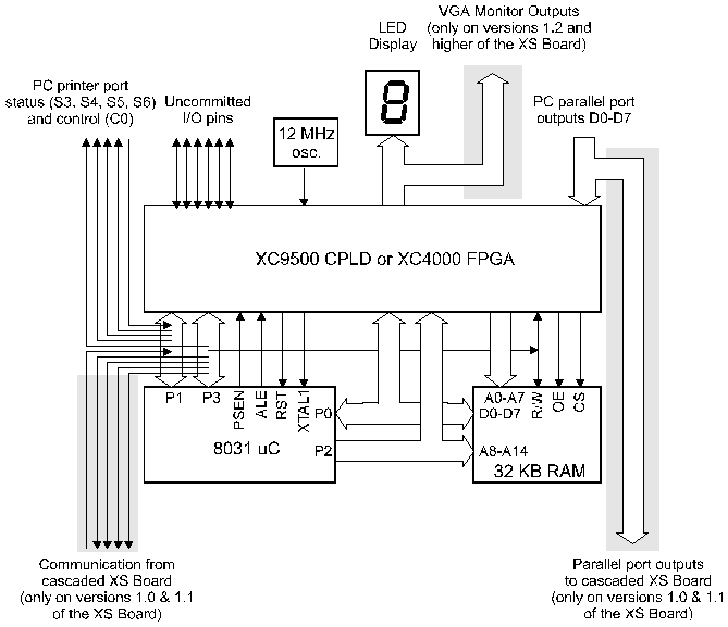
Figure 3: Connections between the 8031 microcontroller, RAM, and
FPLD of the XS Board.
Meanwhile, the upper eight bits of the address are output on port P2 of the 8031. The RAM uses the lower seven of these address bits. The FPLD also receives the upper eight address bits and decodes these along with the PSEN and read/write control line (from pin P3.6 of port P3 ) from the 8031 to generate the CS and OE signals that enable the RAM and its output drivers, respectively. Either of the CS or OE signals can be pulled high to disable the RAM and prevent it from having any effect on the rest of the XS Board circuitry.
One of the outputs of the CPLD controls the reset line of the microcontroller. The 8031 can be prevented from having any effect on the rest of the circuitry by forcing the RST pin high through the FPLD. (When RST is active, most of the 8031 pins are weakly pulled high.)
Many of the I/O pins of ports P1 and P3 of the 8031 connect to the FPLD and can be used for general-purpose I/O between the microcontroller and the FPLD. In addition to being general-purpose I/O, the P3 pins also have special functions such as serial transmitters, receivers, interrupt inputs, timer inputs, and external RAM read/write control signals. If you aren't using a particular special function, then you can use the associated pin for general-purpose I/O between the microcontroller and the FPLD. In many cases, however, you will program the FPLD to make use of the special-purpose 8031 pins. (For example, the FPLD could generate 8031 interrupts.) If you want to use the special-purpose pin with an external circuit, then the FPLD I/O pin connected to it must be tristated.
An LED digit connects directly to the FPLD. (These same FPLD pins also drive the VGA monitor connector on versions 1.2 and higher of the XS Board.) The FPLD can be programmed so the microcontroller can control the LEDs either through P1 or P3 or by memory-mapping a latch for the LED into the memory space of the 8031.
The PC can transmit signals to the XS Board through the eight data output bits of the printer port. The FPLD has direct access to these signals. The microcontroller can also access them by programming the FPLD to pass the data output bits onto the FPLD I/O pins connected to the 8031. The printer port data bits are also passed through the cascade header to the next XS Board in the chain (if there is one).
Communication from the XS Board back to the PC also occurs through the parallel port. Four of the parallel port status pins are connected to three pins of P1 and one pin of P3 . Either the microcontroller or the FPLD can drive the status pins. The PC can read the status pins to fetch data from the XS Board.
Questions:
I´m trying to make a conexion using the target xs40-005xl with a ethernet chip (realtek 8019AS or crystal cs8900A-CQ) and i´m quite loose, any the information you cuold send me for my purpose will be important for me. Thanks for all. I´m sorry but my english is not very good.
| file: /Techref/xess/manual.htm, 38KB, , updated: 2001/6/18 11:27, local time: 2024/7/27 06:28,
18.227.105.83:LOG IN
|
| ©2024 These pages are served without commercial sponsorship. (No popup ads, etc...).Bandwidth abuse increases hosting cost forcing sponsorship or shutdown. This server aggressively defends against automated copying for any reason including offline viewing, duplication, etc... Please respect this requirement and DO NOT RIP THIS SITE. Questions? <A HREF="http://piclist.com/techref/xess/manual.htm"> XS40 and XS95 Board Manual</A> |
| Did you find what you needed? |
|
o List host: MIT, Site host massmind.org, Top posters @none found - Page Editors: James Newton, David Cary, and YOU! * Roman Black of Black Robotics donates from sales of Linistep stepper controller kits. * Ashley Roll of Digital Nemesis donates from sales of RCL-1 RS232 to TTL converters. * Monthly Subscribers: Gregg Rew. on-going support is MOST appreciated! * Contributors: Richard Seriani, Sr. |
Welcome to piclist.com! |
.